Further Boolean Logic and Truth Tables
1) From Truth Tables to Circuits: The 3-Bit Prime Number Detector
In module 1, you learned about basic logic gates (AND, OR, NOT) and how to read a truth table to understand what a circuit does. And, in the previous exercise, you learnt and verified some boolean identities. But what if you want to create a circuit from scratch to solve a specific problem?
We can use truth tables in reverse: we define the behavior we want in a truth table first, and then translate that table into a physical wiring diagram.
Take the following problem, for instance:
Design a circuit which takes a 3-bit positive integer as input and has one bit of output, where the output is HIGH if and only if the input is a prime number.
Step 1: Defining the Truth Table
Since it is a 3-bit input, our possible numbers range from 0 (000) to 7 (111). Let the binary digits be x4, x2, x1 (representing the 4s place, 2s place, and 1s place).
We know the prime numbers between 0 and 7 are 2, 3, 5, and 7. (Note: 0 and 1 are not prime numbers). Therefore, our output y should only be HIGH (1) for those specific decimal values.
Let's draw out the complete truth table. Here, we use H (HIGH/1) and L (LOW/0).

| Decimal | x4 (Fours) | x2 (Twos) | x1 (Ones) | y (Output) | Is it Prime? | ||
|---|---|---|---|---|---|---|---|
| 0 | L | L | L | L | No | ||
| 1 | L | L | H | L | No | ||
| 2 | L | H | L | H | Yes! | ||
| 3 | L | H | H | H | Yes! | ||
| 4 | H | L | L | L | No | ||
| 5 | H | L | H | H | Yes! | ||
| 6 | H | H | L | L | No | ||
| 7 | H | H | H | H | Yes! |
2) Method: Sum of Products (SOP)
How do we turn that table into a physical circuit? We use a universally applicable method called the Sum of Products (SOP).
The strategy is simple:
- Ignore all the rows where the output is LOW (L).
- For every row where the output is HIGH (H), create a mini-equation (called a minterm or a product term) using AND gates that is only true for that specific row.
- Combine all those mini-equations together.
Let's look at the first prime number: 2 (Binary 010). We need a term that outputs HIGH only when x4 is LOW, x2 is HIGH, and x1 is LOW. To achieve this with an AND gate, all inputs going into the AND gate must be HIGH. So, we must invert the LOW signals using NOT gates (represented by prime notation: '). Therefore, our minterm for the number 2 is: x4' · x2 · x1'.
Similarly, the minterm for the number 3 is: x4' · x2 · x1.

Once you find the minterms for all the prime numbers (2, 3, 5, and 7), you will have four separate expressions that each trigger on a specific prime number.
The final unsimplified boolean equation will look like this where any prime number as input will produce a 1 at the output and 0 otherwise:
3) Boolean Simplification: The 3-Bit Prime Generator
Building that 4-term equation on a breadboard as-is would require multiple ICs and a terrifying amount of wiring. Fortunately, we can use the Boolean identities you learned in the previous exercise to simplify this expression into a much smaller, cheaper circuit!
Let's break it down step-by-step using Boolean Algebra.
Step 1: Grouping and Factoring (Distributive Law) Look at the first two terms: (x4'x2x1') and (x4'x2x1). Notice that they both share x4'x2. Let's factor that out:
Now look at the last two terms: (x4x2'x1) and (x4x2x1). These both share x4x1. Factoring that out gives us:
Step 2 & 3: Final Simplification Substitute the result from the question above back into our factored expressions. Then, apply the Identity Law (which states that anything AND'd with 1 is just itself).

4) Scaling Up: The 4-Bit Prime Number Detector
Now let's apply this entire process—Truth Table → SOP Equation → Boolean Simplification → Breadboard Circuit—to extend the circuit to 4-bits and finally implement it on a breadboard.
We are going to construct a 4-Bit Prime Number Detector. Because we are using 4 bits (x8, x4, x2, x1), our circuit will be able to evaluate numbers from 0 all the way to 15!
Here is the full 4-bit Truth Table. Notice that we have left the Output column blank for the bottom half of the table. It is your job to figure out which of those binary values are prime!
| x8 | x4 | x2 | x1 | y (Output) | Is it Prime? |
|---|---|---|---|---|---|
| 0 | 0 | 0 | 0 | 0 | No |
| 0 | 0 | 0 | 1 | 0 | No |
| 0 | 0 | 1 | 0 | 1 | Yes! |
| 0 | 0 | 1 | 1 | 1 | Yes! |
| 0 | 1 | 0 | 0 | 0 | No |
| 0 | 1 | 0 | 1 | 1 | Yes! |
| 0 | 1 | 1 | 0 | 0 | No |
| 0 | 1 | 1 | 1 | 1 | Yes! |
| 1 | 0 | 0 | 0 | ||
| 1 | 0 | 0 | 1 | ||
| 1 | 0 | 1 | 0 | ||
| 1 | 0 | 1 | 1 | ||
| 1 | 1 | 0 | 0 | ||
| 1 | 1 | 0 | 1 | ||
| 1 | 1 | 1 | 0 | ||
| 1 | 1 | 1 | 1 |
If you did that correctly, you found two more prime numbers in that bottom half! Let's write out the full unsimplified Sum of Products for all six prime numbers in our 4-bit system. We will label these six minterms T_A through T_F:
5) Advanced Simplification: Extending the 3-Bit Circuit
To simplify this complex 4-bit logic, we don't need to start from scratch. Notice that for the first half of our truth table (numbers 0 through 7), the x8 bit is always 0 (x8').
Because the prime numbers in this range (2, 3, 5, 7) are identical to our previous 3-bit problem, we can simply take our fully simplified 3-bit equation (y = x4'x2 + x4x1) and AND it with x8'!
This gives us the equation for the first half of our table:
Now, we only have to worry about the second half of the table where x8 is 1 (numbers 8 through 15). The only prime numbers here are 11 and 13.
Let's write down their specific product terms (minterms):
- 11 (1011): x8x4'x2x1
- 13 (1101): x8x4x2'x1
Combining the two halves together, our complete unsimplified 4-bit prime number equation is:
This is better than a 6-term equation, but we can simplify it even further by grouping terms that share common variables. Let's pair the 1st term with the 3rd term, and the 2nd term with the 4th term:
- Pair A: x8'x4'x2 + x8x4'x2x1
- Pair B: x8'x4x1 + x8x4x2'x1
Let's factor out the common variables in Pair A (x4'x2):
Applying this rule to both pairs:
- Pair A simplifies to: x4'x2(x8' + x1)
- Pair B factors to x4x1(x8' + x8x2'), which simplifies to: x4x1(x8' + x2') = x4x1(x8x2)' using De Morgan's law.
By combining our fully simplified pairs, we get the following equation:
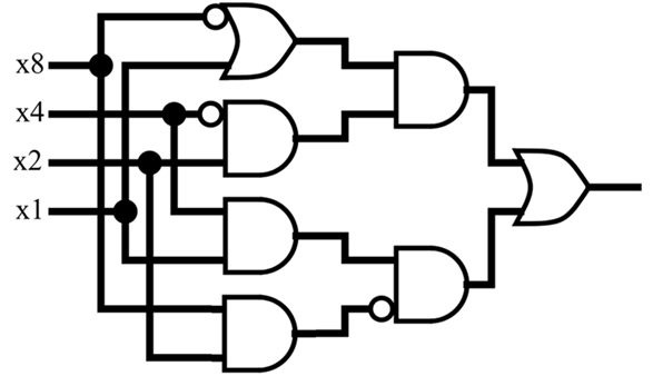
6) Hardware Implementation: Building the 4-Bit Detector
We are going to build this optimized equation on your breadboard. Let's look at the components required based on our factored mathematical simplification:- NOT Gates: We need to invert x8 and x4, plus one more NOT gate to invert the (x8x2) product.
- AND Gates: We need them to form the individual products (like x4'x2) and to multiply the grouped terms in our two main branches.
- OR Gates: We need one to evaluate the (x8' + x1) term, and a final one to sum the two main branches together.
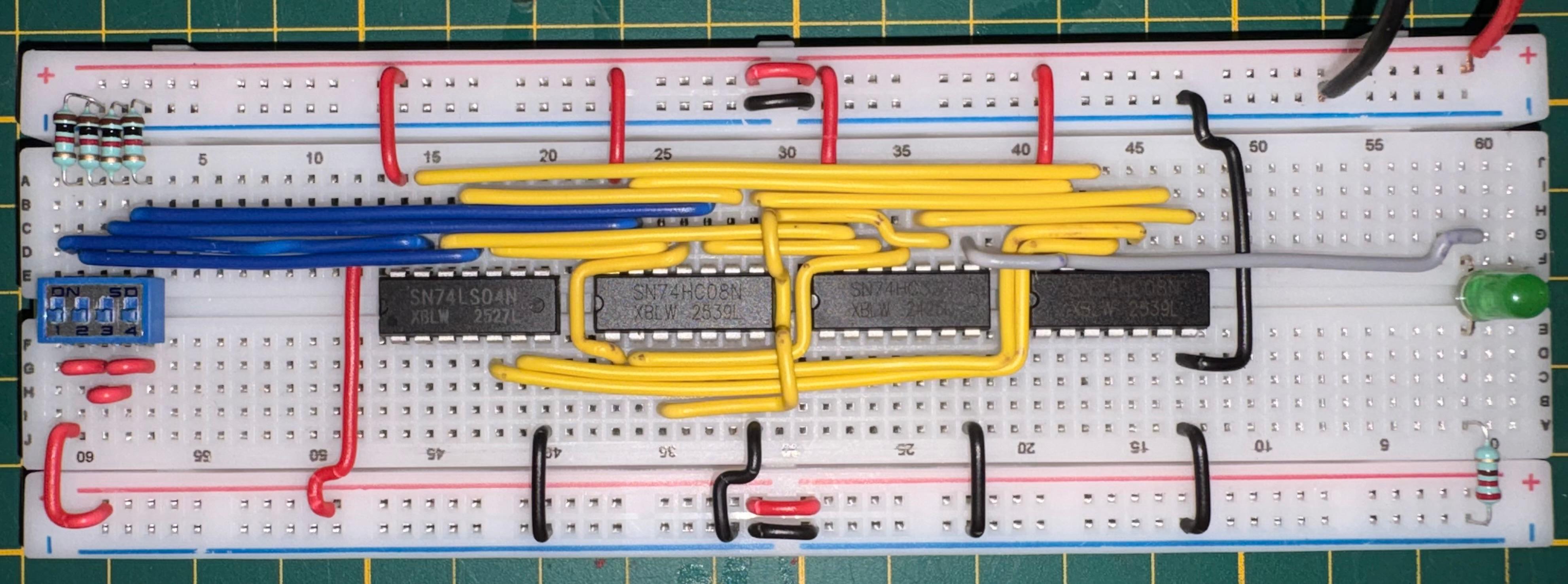
Components You'll Need
- 1x 7404 Hex Inverter (NOT Gates)
- 2x 7408 Quad 2-Input AND Gate
- 1x 7432 Quad 2-Input OR Gate
- 4x DIP Switches (for inputs x8, x4, x2, x1)
- 1x LED and 220Ω Resistor
General Design Instructions
Use the provided pinout diagrams and your factored boolean equation to wire up the breadboard.
1.  **Power & Ground:** Start by connecting VCC to 5V and GND to Ground for all four ICs. Set up four DIP switches to represent $x8, x4, x2, x1$.
2.  **Initial Inversions:** Route your $x8$ and $x4$ switches into the 7404 Hex Inverter to generate the $x8'$ and $x4'$ signals.
3.  **Top Branch $x4'x2(x8' + x1)$:** * Route $x8'$ and $x1$ into an OR gate.
    * Route $x4'$ and $x2$ into an AND gate.
    * Route the outputs of those two gates into a third AND gate.
4.  **Bottom Branch $x4x1(x8x2)'$:** * Route $x4$ and $x1$ into an AND gate.
    * Route $x8$ and $x2$ into an AND gate, then pass its output directly through a NOT gate to invert it.
    * Route the outputs of these two gates into a third AND gate.
5.  **Final Sum:** Route the final outputs of your top and bottom branches into your 7432 OR gate IC to sum them together.
6.  **Final Output:** Connect the final OR gate output to an LED with a 220Ω resistor.
When you toggle your switches, your LED will now perfectly evaluate your logic and light up ONLY if you input the binary equivalents of 2, 3, 5, 7, 11, or 13!
Summary & What's Next
- You defined the desired behavior using a Truth Table.
- You converted that table into a boolean equation using the Sum of Products (SOP) method.
- You simplified complex equations mathematically using the Idempotent Law to duplicate terms.
- You mapped those equations to physical hardware gates across 4 different ICs to build a functional 4-Bit Prime Number Detector.
In the next exercise, we'll learn about multiplexers and demultiplexers.