Boolean Algebra
1) Boolean Algebra & Simplification
Boolean algebra, named after the 19th century English mathematician George Boole, is a branch of algebra where we use only two values. For our purposes, these are HIGH and LOW or 1 and 0. These are often also denoted as TRUE and FALSE.
In the previous sections, we looked at some basics, and we will now see how we can use some rules of boolean algebra to simplify things.
Some Notation:
We will be treating our inputs and outputs as variables: x, y, z, a, b, c etc. Each variable can take a value of 1 or 0. We will represent each gate with a symbol. a EQUALS b can be denoted a ≡ b. Additionally:
- NOT a ≡ a' (Read as "a prime")
- a AND b ≡ a · b ≡ ab
- a OR b ≡ a + b
- a XOR b ≡ a ⊕ b
Simpler expressions can be used to express more complicated expressions:
- x ⊕ y ≡ x y' + x' y
2) Hands-On: Verifying Identities
For each of the following, predict what the output will be. Then, build and verify each circuit.
Hardware Setup: Place your 7408 (AND), 7432 (OR), and 7404 (NOT) ICs on your breadboard. Connect VCC (Pin 14) to the 5V rail and GND (Pin 7) to the Ground rail for all chips. Use DIP switches for your variable a, and an LED (with a 220Ω resistor) to read the output.
Activity 1: Connect Pin 1 of the 7408 (AND gate) to your switch a, and Pin 2 directly to Ground (0). Connect Pin 3 (Output) to your LED. Flip the switch— how does the LED behave? Test the other configurations below by swapping connections to Ground (0) or VCC (1) on the AND and OR gates.
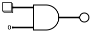


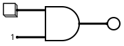
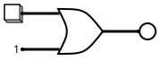
Explanation: The circuits you just built demonstrate the Annulment and Identity laws of Boolean algebra. For an AND gate, connecting one input to 0 always outputs 0 (Annulment: a · 0 ≡ 0), while connecting to 1 outputs the variable itself (Identity: a · 1 ≡ a). For an OR gate, connecting one input to 1 always outputs 1 (Annulment: a + 1 ≡ 1), while connecting to 0 outputs the variable itself (Identity: a + 0 ≡ a).
Activity 2: Wire your single switch a to both inputs of an AND gate (Pins 1 and 2 on the 7408). Repeat this for both inputs of your OR gate.
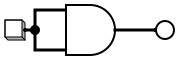
Explanation: This demonstrates the Idempotent laws. ANDing or ORing a variable with itself simply results in the variable itself (a · a ≡ a and a + a ≡ a).
Activity 3: Connect switch a to Pin 1 of your OR gate (7432). Also connect switch a to Pin 1 of your NOT gate (7404). Then, take the NOT output (Pin 2) and connect it to the other OR input (Pin 2). Repeat this setup using the AND gate. Finally, pass the switch through two NOT gates in a row.
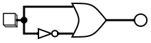

Explanation: You verified the Complement laws and Double Negation. ANDing a variable with its complement always yields 0 (a · a' ≡ 0) because they can never both be HIGH. ORing them always yields 1 (a + a' ≡ 1) because one of them will always be HIGH. Passing a signal through two NOT gates just returns the original signal ((a')' ≡ a).
Activity 4: Connect switch a to one input of an OR gate, and switch b to the other. Then, feed the output of that OR gate into an AND gate, along with a separate wire from switch a. Do the opposite for the second circuit below.
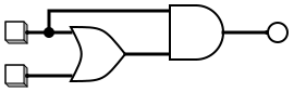
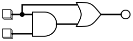
Explanation: These circuits demonstrate the Absorption laws. A complex expression like a · (a + b) or a + ab simply absorbs the second variable (b), effectively returning just a in all cases!
Note that these exercises are all about simplifying circuits. We previously looked at ways to create a circuit given a truth table, and now we can simplify the circuits we made. The following two exercises are about what are known as De Morgan's laws:
Activity 5:
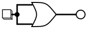
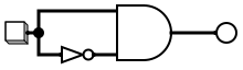
- Left Side: Build a NOR gate using a 7432 (OR) fed into a 7404 (NOT). Connect switches a and b to the inputs. Connect the output to LED 1.
- Right Side: Pass switches a and b through separate NOT gates (7404). Connect those inverted signals into a 7408 (AND). Connect the output to LED 2.
- Toggle your switches through all 4 combinations (00, 01, 10, 11). Do LED 1 and LED 2 always match?
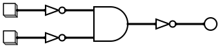
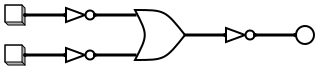
Explanation: You verified De Morgan's Laws. A NOR gate is logically equivalent to an AND gate with inverted inputs. A NAND gate is equivalent to an OR gate with inverted inputs.
The table below summarizes the activities you have done so far in this exercise. Just like standard math, there are identities that help us simplify complex expressions into smaller, cheaper circuits.
| Rule Type | AND (·) | OR (+) |
|---|---|---|
| Annulment | a · 0 ≡ 0 | a + 1 ≡ 1 |
| Identity | a · 1 ≡ a | a + 0 ≡ a |
| Idempotent | a · a ≡ a | a + a ≡ a |
| Complement | a · a' ≡ 0 | a + a' ≡ 1 |
| Double Negation | (a')' ≡ a | |
| Absorption | a · (a + b) ≡ a | a + a · b ≡ a |
| De Morgan's | (a · b)' ≡ a' + b' | (a + b)' ≡ a' · b' |
| Commutativity | a · b ≡ b · a | a + b ≡ b + a |
| Associativity | a · (b · c) ≡ (a · b) · c | a + (b + c) ≡ (a + b) + c |
| Distributivity | a · (b + c) ≡ a · b + a · c | a + b · c ≡ (a + b) · (a + c) |
In the next exercise, we'll learn more on boolean logic and truth tables.