Multiplexers and Demultiplexers
In the previous exercise, you constructed a 4-bit prime number detector by deriving a complete Sum of Products (SOP) expression and simplifying it via Boolean algebra. While mathematically rigorous, implementing such high-variable logic with individual gates often leads to high component counts and complex wiring on a breadboard.
1) Multiplexers (MUX)
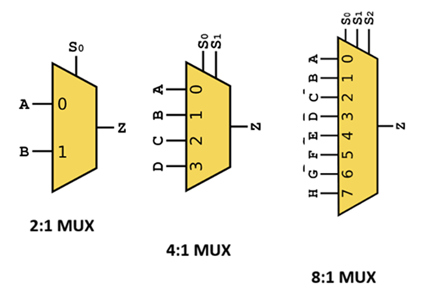
An n-bit multiplexer has the following function: Given 2^n 1-bit inputs and one n-bit "select" input, it provides one 1-bit output. If the n-bit input is x, then the output is equal to the x^{th} 1-bit input. More simply, a multiplexer takes several inputs and a selection number, then forwards the input at that position to the output.
The most fundamental unit is the 2:1 Multiplexer. It features two data inputs (a and b) and one select bit (s).
The operation of a 2:1 MUX is defined by the following Boolean equation: o = (s' \cdot a) + (s \cdot b)
| s (Select) | a (Input 0) | b (Input 1) | o (Output) |
|---|---|---|---|
| L | L | L | L |
| L | L | H | L |
| L | H | L | H |
| L | H | H | H |
| H | L | L | L |
| H | L | H | H |
| H | H | L | L |
| H | H | H | H |
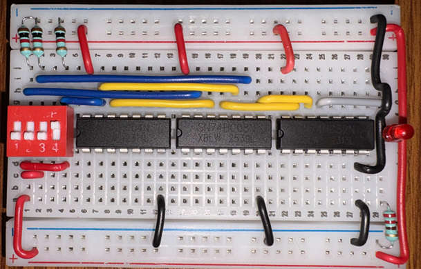
Activity: Building a 2:1 Multiplexer
To understand the internal logic of a data selector, you will build a 2:1 MUX using discrete logic gates.
Components needed:
- 1x Breadboard
- 1x 74LS08 (Quad 2-input AND gate)
- 1x 74LS32 (Quad 2-input OR gate)
- 1x 74LS04 (Hex Inverter/NOT gate)
- LEDs and 330\Omega resistors for output visualization
- Jumper wires and power supply
Step-by-step design guide:
- Power the ICs: Place the 74LS04, 74LS08, and 74LS32 on your breadboard. Connect Pin 14 of each to VCC (5V) and Pin 7 to GND.
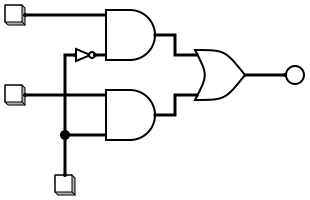
- Invert the Select Line: Connect your select signal (s) to the input of a NOT gate (Pin 1 of 74LS04). The output (Pin 2) is now s'.
- Implement the AND terms: * Connect s' (from Pin 2 of 74LS04) and input a to the first AND gate (Pins 1 and 2 of 74LS08).
- Connect the direct select signal s and input b to the second AND gate (Pins 4 and 5 of 74LS08).
- Final Summation: Connect the outputs of the two AND gates (Pins 3 and 6 of 74LS08) to the inputs of an OR gate (Pins 1 and 2 of 74LS32).
- Verify: Connect the OR gate output (Pin 3 of 74LS32) to an LED. Test all four combinations of a and b for both s=0 and s=1 to match the truth table.

2) Demultiplexers (DEMUX)
A demultiplexer does the exact opposite of a multiplexer. Given one n-bit select input and one 1-bit data input, it provides 2^n 1-bit outputs. If the n-bit select input is x, then the x^{th} output is equal to the 1-bit data input, and all other outputs are LOW.
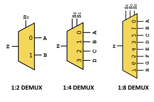
Hence, we can construct the following truth table for a 1:2 demultiplexer:
| s (Select) | i (Input) | a (Output 0) | b (Output 1) |
|---|---|---|---|
| L | L | L | L |
| L | H | H | L |
| H | L | L | L |
| H | H | L | H |
3) Partitioning for the Prime Detector
A powerful application of multiplexers is "function implementation by partitioning." We can implement the 4-bit prime detector by using the Most Significant Bit (MSB), x_8, as the select pin (s) for a 2:1 MUX. This effectively splits the 16-row truth table into two 8-row sub-problems. When x_8 = 0, the MUX selects the logic for numbers 0–7. When x_8 = 1, it selects the logic for numbers 8–15.
Partition 1 (x_8 = 0): Numbers 0-7 The prime numbers in this range are 2, 3, 5, and 7.
| x_4 | x_2 | x_1 | Output (y) |
|---|---|---|---|
| 0 | 0 | 0 | 0 |
| 0 | 0 | 1 | 0 |
| 0 | 1 | 0 | 1 |
| 0 | 1 | 1 | 1 |
| 1 | 0 | 0 | 0 |
| 1 | 0 | 1 | 1 |
| 1 | 1 | 0 | 0 |
| 1 | 1 | 1 | 1 |
Partition 2 (x_8 = 1): Numbers 8-15 The prime numbers in this range are 11 (1011_2) and 13 (1101_2).
| x_4 | x_2 | x_1 | Output (y) |
|---|---|---|---|
| 0 | 0 | 0 | 0 |
| 0 | 0 | 1 | 0 |
| 0 | 1 | 0 | 0 |
| 0 | 1 | 1 | 1 (Decimal 11) |
| 1 | 0 | 0 | 0 |
| 1 | 0 | 1 | 1 (Decimal 13) |
| 1 | 1 | 0 | 0 |
| 1 | 1 | 1 | 0 |
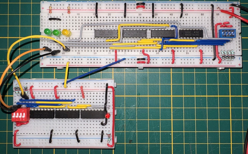
Activity: 4-Bit Prime Detector Integration
Let's design the same 4-bit prime number detector you designed in the previous exercise using MULTIPLEXER that you just designed, and the 3-bit prime number detector along with some more gates.
Components needed:
- Your existing 3-bit prime detector circuit (from Partition 1)
- New logic gates for Partition 2 (1x 74LS86 XOR gate and 1x 74LS08 AND gate to detect 11 and 13)
- The 2:1 MUX circuit built in the previous activity
- Four input switches (x_8, x_4, x_2, x_1)
Step-by-step design guide:
- Prepare Logic Outputs:
- Ensure your 3-bit prime detector output (from previous module) is ready to serve as input a for the MUX.
- Implement logic for Partition 2: The unsimplified expression for 11 and 13 is y = x_4'x_2x_1 + x_4x_2'x_1, which simplifies to y = (x_4 \oplus x_2) \cdot x_1. This uses an XOR gate and an AND gate to detect 1011 and 1101 when the MSB is assumed to be 1. This output will serve as input b for the MUX.
- Connect to MUX: * Wire the output of Partition 1 to MUX Input a.
- Wire the output of Partition 2 to MUX Input b.
- Assign the Select Line: Use the x_8 switch as the select bit (s) for the MUX.
- Final Test: Switch through all 16 binary inputs. The final LED at the MUX output should only light up for primes: 2, 3, 5, 7, 11, and 13.
Next, we will build an 7 segment display decoder from scratch using the concepts learnt in the module.