Binary to 7-segment Display Decoder
In this project, you will be designing a circuit you will use fairly often in this course—a binary to 7-segment display decoder. Because of the complexity and tedium of building a complete version of this circuit (going from 0 to 9), we will be building a simplified version. This one will only decode numbers from 0 to 5.
Here, we will introduce some new notation: X. In a truth table, this denotes a value which does not matter to the functioning of the circuit. In particular, we will be using this for input numbers greater than 5.
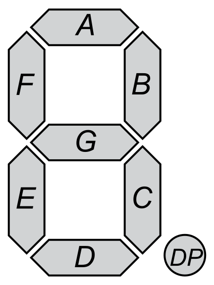
For this project, we will be creating separate circuits with each segment of the 7-segment display, since they are all somewhat independent of each other. First, let us name the segments. Typically, each of the seven segments are labelled one of a,b,c,d,e,f,g. In most single 7-segment displays, there is also a decimal point, which we will ignore for this circuit. In the diagram below, the decimal point is labelled DP.
1) Project Activity: Mapping the Decoder
Based on the segment mapping above, determine which segments must be HIGH (lit up) for each decimal number. Select the checkboxes for the segments that should be active.
Decimal: 0 (Binary: 000)

Decimal: 1 (Binary: 001)
Decimal: 2 (Binary: 010)
Decimal: 3 (Binary: 011)
Decimal: 4 (Binary: 100)
Decimal: 5 (Binary: 101)
Now that you have mapped the intended behavior for segments a through g, the next step is to derive the boolean expressions for each segment so we can build the actual hardware decoder!
Use all the techniques you have learnt to create a this circuit.
2) Decoder Design for Decimal 0 to 5
To start with, notice that a\equiv d. This means that we only need to design circuits for six of the segments. So, let us take a look at them one at a time.
a)
| x_4 | x_2 | x_1 | a | |
|---|---|---|---|---|
| L | L | L | H | |
| L | L | H | L | |
| L | H | L | H | |
| L | H | H | H | |
| H | L | L | L | |
| H | L | H | H | |
| H | H | L | X | |
| H | H | H | X |
For this one, we can see that there are four rows for which a=H, and hence two rows for which a=L. Because of this, we can come up with an expression which is LOW only for those two rows (similar to what we did in the previous section)
- a' \Leftarrow x_1 \cdot x_2' \cdot x_4'
- a' \Leftarrow x_4 \cdot x_2' \cdot x_1'
Inverting each of these and connecting them with an AND:
- a \equiv (x_1 \cdot x_2' \cdot x_4')' \cdot (x_4 \cdot x_2' \cdot x_1')'
Simplifying using de Morgan's law:
- a \equiv ((x_1 \cdot x_2' \cdot x_4') + (x_4 \cdot x_2' \cdot x_1'))'
By distributivity:
- a \equiv (x_2' \cdot (x_1 \cdot x_4' + x_4 \cdot x_1'))'
Take note of the expression x_1 x_4' + x_1' x_4; we have been using a similar expression.
This is identical to the definition of \oplus. Thus:
- a \equiv (x_2' \cdot (x_1 \oplus x_4))'
By de Morgan's law:
- a \equiv x_2 + (x_1 \oplus x_4)'
This is about as simplified we are going to be able to get it, so we can stop here. This expression will use three gates—one XOR gate, one OR gate, and one NOT gate.
b)
| x_4 | x_2 | x_1 | b | |
|---|---|---|---|---|
| L | L | L | H | |
| L | L | H | H | |
| L | H | L | H | |
| L | H | H | H | |
| H | L | L | H | |
| H | L | H | L | |
| H | H | L | X | |
| H | H | H | X |
Here we only have one row where b \equiv L. From this we get:
- b' \equiv x_4 \cdot x_2' \cdot x_1
We cannot simplify it further. Using de Morgan's law gets us the following:
- b \equiv x_4' + x_2 + x_1'
This highlights one problem with this approach: When there are don't care (X) conditions, this method does not yield the minimal expression. Right now, there are two don't care conditions, and so there are four possible expressions, each for a different combination of values of X. In this case, we can find the minimal expression with brute force. This will not work, however, for truth tables with more X conditions. In this case, there is at least one minimal solution that is constructible using only two logic gates from AND, OR, XOR, NAND, NOR, NOT (Note that they need not be two different gates)
c)
This row has a solution with one gate.
Hint
One of the three inputs does not matter here.
d)
Hint
This question is just checking if you have been paying attention so far. This should be trivial if you have been.
e)
Here, there is a solution with two logic gates.
f)
This will require two logic gates.
g)
g can be expressed using only one logic gate.
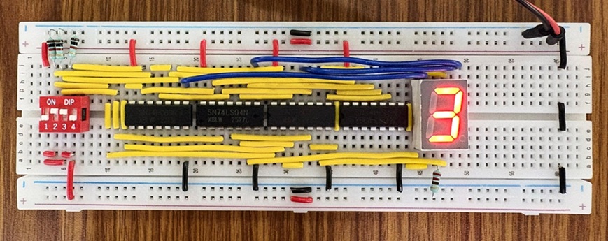
3) Hands-On: Building the Decoder
Now that you have derived the minimal boolean expressions for all seven segments, it's time to build the actual hardware decoder! You will use standard logic gate ICs to calculate the states for segments a through g simultaneously, and output those signals to a physical 7-segment display.
Since this circuit involves calculating 7 different logic equations from the same 3 inputs, your breadboard will get crowded quickly. Take your time, cut your wires neatly, and color-code your inputs (x_4, x_2, x_1) versus your outputs (a through g).
Components You'll Need:
- 1x 7-Segment Display (Common Cathode recommended)
- Logic Gate ICs: 7404 (NOT), 7408 (AND), 7432 (OR), and 7486 (XOR)
- 1x 3-position DIP switch
- 7x 220Ω Resistors
- Breadboard & Jumper wires
Step-by-Step Design:
- Power & Ground: Place your logic ICs onto the breadboard straddling the center gap. Connect VCC (Pin 14) to the 5V rail and GND (Pin 7) to the ground rail for all ICs.
- Setup Inputs: Connect your 3-position DIP switch to create inputs x_4, x_2, and x_1. Route these three main input lines down a dedicated row or bus on your breadboard so you can easily tap into them for multiple gates.
- Wire the Inverters: Since many of your equations likely require x_1', x_2', or x_4', pass your main inputs through the 7404 Hex Inverter first. Keep these inverted signals accessible.
- Build the Logic (Segment by Segment): * Go through your derived equations one by one (from a to g).
- Use the 7408 (AND), 7432 (OR), and 7486 (XOR) gates to build the expression for each segment.
- Pro-Tip: If two segments share the exact same equation (like a and d), you don't need to build the circuit twice! Just run two wires from the final output gate.
- Connect to the Display: * Place your 7-segment display on the breadboard. If it is a Common Cathode display, connect the common pins (usually the middle pins on top and bottom) to Ground.
- Connect the output of your logic circuit for segment a to the a pin on the display through a 220Ω resistor.
- Repeat this for segments b through g.
- Test & Verify: Turn on your power supply. Toggle your DIP switches from
000to101. You should see the digits 0, 1, 2, 3, 4, and 5 successfully render on your display!