Basics of Latches
So far, the circuits you have built using logic gates fall under combinational logic. In combinational circuits, the outputs depend only on the current inputs; there is no stored state (no memory element).
Let's try to understand this difference with a simple example:
- Push button (combinational): Pressing the button turns the light ON; releasing it turns the light OFF. The output changes only while the input is applied.
- Toggle switch (sequential): Activating the switch changes the state and the light remains ON until the next interaction. The system retains its previous state.
In sequential logic, the next output depends on both the current inputs and the current state (stored information from the past). In this section, you will design circuits that store a single bit. The most fundamental storage element is the latch.
Module 3 covers Combinational Logic in depth.
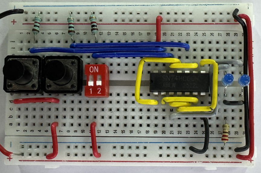
1) Hardware Setup: The 7400 IC
Before analyzing latch behavior, set up your breadboard using the 7400 Quad 2-Input NAND Gate IC.

Components Needed:
- 1x 7400 IC (NAND Gates)
- 2x Push Buttons (for Set/Reset)
- 2x LEDs (Red and Green)
- Resistors (330Ω for LEDs, 10kΩ for pull-up/down)
Important Wiring Note: The 7400 IC contains four separate NAND gates.
- Gate 1: Pins 1, 2 (Inputs), 3 (Output)
- Gate 2: Pins 4, 5 (Inputs), 6 (Output)
- Gate 3: Pins 9, 10 (Inputs), 8 (Output)
- Gate 4: Pins 12, 13 (Inputs), 11 (Output)
- Power: Pin 14 (VCC +5V), Pin 7 (GND)
2) The "Memory" Circuit: SR Latch
You are about to build a basic memory element: the SR latch. Unlike combinational circuits, a latch can retain its output state even after the input stimulus is removed.
In the diagrams below, notice the cross-coupled wiring: the output of the top NAND gate feeds one input of the bottom NAND gate, and the output of the bottom NAND gate feeds one input of the top NAND gate. This cross-coupling is called feedback, and it is what enables storage.
For a NAND gate, any input of 0 forces the output to 1. The output is 0 only when both inputs are 1.
Phase 1: Turning it ON (The "Set" Action)
Assume the circuit is currently in the OFF state. The goal is to drive it to the ON state and have it remain there after the input returns to its inactive level. This is done using the top switch (Set path).
 1. Starting State (OFF)
Q is OFF. Both switches are in their default (inactive) positions.
1. Starting State (OFF)
Q is OFF. Both switches are in their default (inactive) positions.
 2. We Press Top Switch
We drive the top input to 0.
2. We Press Top Switch
We drive the top input to 0. The top NAND gate therefore outputs 1, and the output (Q) changes accordingly.
 3. We Release the Switch
We release the switch (it returns to 0).
3. We Release the Switch
We release the switch (it returns to 0). Q remains ON because feedback maintains the stored state. The circuit has latched the value.
Why does it retain the state?
In Step 2, when the top gate output becomes 1, that value drives the bottom gate’s input. With both of the bottom gate’s inputs at 1, the bottom gate outputs 0. That 0 is fed back into the top gate, which forces the top gate output to remain 1 even after the external switch returns to 1. The loop therefore stabilizes in a consistent state.
Phase 2: Turning it OFF (The "Reset" Action)
Now the latch is in the ON state. To drive it to the OFF state, assert the bottom switch (Reset path) to force the opposite stable state.
1. Starting State (ON)
Q is ON due to the previously stored state. Feedback maintains this state.
 2. We Press Bottom Switch
We drive the bottom input to 1.
2. We Press Bottom Switch
We drive the bottom input to 1. The bottom NAND gate therefore forces its output to 1.
3. We Release the Switch
That 1 is fed into the top gate. The top gate now sees two 1s and therefore outputs 0. Q turns OFF and remains OFF due to feedback.

3) Controlled Updates: Enable-Gated SR Latch
The basic SR latch can change state whenever its inputs change. In practical digital systems, memory elements are typically allowed to update only under controlled conditions. A common approach is to add an enable input so the latch responds to Set/Reset only when the system permits it.
Hardware Implementation: Implement this by using the remaining two NAND gates on the 7400 (Gates 3 and 4) as input-gating stages. Their outputs drive the inputs of the inner SR latch.
4) Scenario 1: Enabled Operation (Enable = 1)
First consider operation when the middle switch (Enable) is ON (Enable = 1). In this condition, the gating stage allows Set and Reset to propagate to the inner latch.
 1. Turning it ON (Set)
Enable is 1. We flip Top Switch to 1.
1. Turning it ON (Set)
Enable is 1. We flip Top Switch to 1.The top gating NAND gate sees two 1s and outputs 0. That 0 drives the inner latch, forcing Q ON.
 2. Memory Mode
We return the top switch to its inactive level.
2. Memory Mode
We return the top switch to its inactive level. The inner latch retains the ON state via feedback, so Q remains ON even after the button is released.
 3. Turning it OFF (Reset)
Enable is 1. We flip Bottom Switch to 1.
3. Turning it OFF (Reset)
Enable is 1. We flip Bottom Switch to 1.The bottom gating NAND gate sees two 1s and outputs 0. That 0 drives the inner latch, forcing Q OFF.
5) Scenario 2: Disabled Operation (Enable = 0)
Now consider the case where Enable is OFF (Enable = 0). In this condition, the gating stage prevents changes at Set/Reset from reaching the inner latch.
 1. The "Shield" is Up
Start Point: The Memory is ON.
1. The "Shield" is Up
Start Point: The Memory is ON. The Guard (Enable) is 0.
The gating stage blocks input changes. The inner latch continues to hold the stored ON state.
 2. Attempting a Reset (Ignored)
We flip the bottom switch to Reset (1) to try and turn Q off.
2. Attempting a Reset (Ignored)
We flip the bottom switch to Reset (1) to try and turn Q off.Result: no change.
Because Enable is 0, the reset signal is blocked and the latch remains ON.
6) Scenario 3: Enable Pulsing for a Controlled State Update
In the previous scenario, Reset had no effect because Enable was low. To allow a state update, Enable must be asserted briefly. A short transition of Enable from 0 to 1 and back to 0 is commonly called a pulse.
3. The Guard Wakes Up
We flip the Enable switch to 1.The gating stage becomes transparent.
The Reset signal (1) is allowed through, the inner latch transitions, and Q turns OFF.
 4. Locked Safely Again
We flip Enable back to 0.
4. Locked Safely Again
We flip Enable back to 0.The gating stage closes again. The latch is protected from further input changes and now retains the new OFF state.
7) Final Project: Build a Gated Latch
For your final submission in this section, you will wire up the Gated SR Latch using your 7400 IC on the breadboard.
Instructions:
- Wire the 4 NAND gates as shown in the logic diagrams above.
- Use a Push Button for the Enable pin.
- Connect an LED (Red) to the main output (let's call it Q).
- Connect a second LED (Green) to the other output of the inner latch (let's call it Q' or Q-bar).
Experiment: Set the latch to ON, then set it to OFF, and observe both LEDs.
In the next section, you will extend this circuit into a D flip-flop, a standard building block used in counters and registers.