Exploring 74181 ALU IC
So far, we have built arithmetic hardware by wiring together adders, registers, and multiplexers.
However, in many real systems, all of these arithmetic and logical functions are bundled into a single chip called an Arithmetic Logic Unit (ALU).
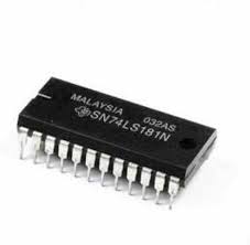
One classic example of such a chip is the 74181 ALU IC.
This device was widely used in early computers and can perform a variety of arithmetic and logical operations depending on how its control pins are configured.
Just like before, instead of directly giving you every connection, we will practice learning from a datasheet.
Take a look at the 74181’s datasheet
At first glance, it may seem overwhelming, but for building basic circuits, the first few pages usually contain everything we need.
For now, we will focus on two major parts of the datasheet.
1) Functionality Overview
Near the beginning of the datasheet, you should find a descriptive section explaining what the ALU does in words.
This section typically tells you:
- What kinds of operations the chip can perform
- How many bits wide the inputs are
- What control signals are used to select functions
Reading this paragraph carefully gives you a high-level understanding of how the ALU behaves before you wire anything.
2) Pinout

Further down on the first few pages, you should find a pinout diagram showing the physical layout of the chip and labeling each pin with its function.
Look for a rectangular drawing of the IC with numbered pins and names beside them.

Now that we know how to locate the 74181’s pinout, let’s broadly categorize its pins.
Input Pins: These pins allow us to provide data and control information to the ALU so it can perform operations.
VCC (pin 24): Positive supply voltage, connect to 5V.
GND (pin 12): Ground reference.
A0–A3 (pins 2, 23, 21, 19): First 4-bit operand inputs.
B0–B3 (pins 1, 22, 20, 18): Second 4-bit operand inputs.
S0–S3 (pins 9–12 depending on package): Function select pins that choose the operation.
M (pin 4): Mode select pin — arithmetic or logic mode.
Cin (pin 7): Carry-in for arithmetic operations and cascading devices.
Output Pins: These pins provide the results of the selected operation and status information.
F0–F3 (pins 5, 6, 8, 10): 4-bit result outputs.
Cout (pin 15): Carry-out from arithmetic operations.
P and G (pins 16 and 17): Propagate and generate outputs for fast carry logic.
A = B (pin 14): Indicates when both inputs are equal.
3) Functions and Select-Line Patterns in the 74181
If you continue reading the 74181’s datasheet, you will find a large table that lists all of the arithmetic and logic functions the chip can perform, along with the exact patterns required on the Mode pin (M) and the four select pins S0–S3.
This table below has all of the functions summarized from the datasheet

In the datasheet, this table is shown alongside the internal logic symbols for the chip, clearly linking each combination of control pins to a mathematical or logical equation
Notice how:
- When M = 0, the chip operates in arithmetic mode, producing sums, differences, increments, and decrements.
- When M = 1, the chip switches to logic mode, producing bit-wise Boolean functions like AND, OR, XOR, and complements.
- The four select pins S0–S3 dramatically expand what the chip can do—five control inputs together allow dozens of unique operations.
Note: Because the 74181 supports such a wide range of functions, it requires many more select pins than the simple add/subtract circuit you built earlier.
In your own design, a single MUX select line chose between two operations.
Inside the 74181, a much larger network of multiplexers and control logic is hidden within the IC, allowing dozens of internal paths to be chosen based on S0–S3 and M.
As you study this table, try to mentally map it onto the blocks you already understand:
- The adder core corresponds to the ripple-carry adders you wired before.
- The increment and subtract modes rely on internal complementing and carry-in paths, just like your 2’s-complement generator plus adder.
- The logic functions come from networks of gates feeding into multiplexers before the final output stage.
Thinking about the chip in this way will help you treat the 74181 not as a mysterious black box, but as a dense packaging of the same fundamental components you have been building throughout the course.
4) Understanding ALU with circuit
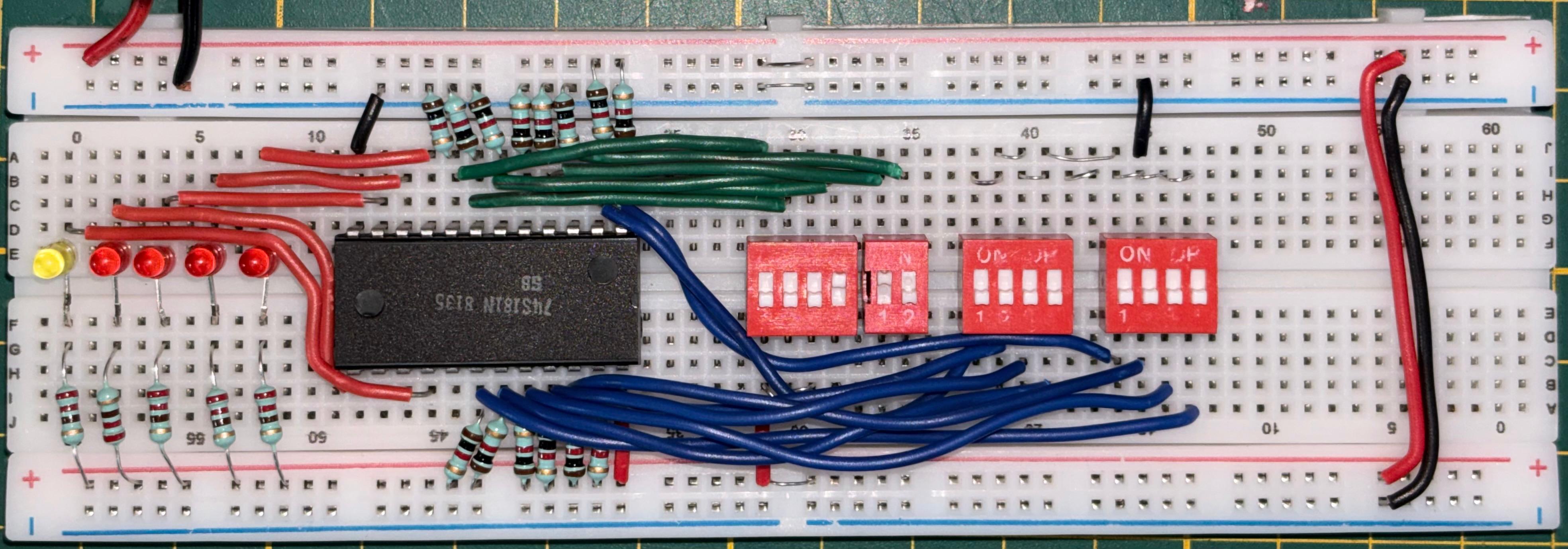
Since, in the previous section, we already designed an Arithmetic Unit of our own, let's verify the functionality by comparing the outputs of the ALU IC to our circuit.
Components you'll need:
- 1x 74181 4-bit ALU IC
- 2x 4-position DIP switches (for Data Inputs A0-A3 and B0-B3)
- 1x 4-position DIP switch (for Function Select Inputs S0-S3)
- 2x 1-position DIP switch or push buttons (for Mode M and Carry-in Cn)
- 5x LEDs
- 5x 220Ω Resistors (for LEDs)
- 6x 1kΩ Resistors (Pull-down for S0-S3, M, Cn)
- 8x 10kΩ Resistors (Pull-up for A0-A3, B0-B3)
- Breadboard & Jumper wires
Step-by-step design:
1. Power & Ground: Place the 74181 IC on the breadboard. Connect VCC (Pin 24) to 5V and GND (Pin 12) to Ground.
2. Wire Control Pins (Active High Logic): Connect the switches for S0-S3, M, and Cn to the 5V rail. Connect the other side of these switches to their respective pins on the IC. Add 1kΩ pull-down resistors from these pins to Ground. When a switch is closed, the input is HIGH.
3. Wire Data Inputs (Active Low Logic): Connect the switches for A0-A3 and B0-B3 to Ground. Connect the other side of these switches to the respective A and B pins on the IC. Add 10kΩ pull-up resistors from these pins to 5V. When a switch is closed, the pin goes LOW (Active).
4. Wire Outputs (Active Low Logic): Connect the cathodes (short legs) of your 5 LEDs to F0-F3 and Cn+4. Connect the anodes (long legs) to 5V through 220Ω resistors. Because the outputs are active low, the LED will turn ON when the output pin is driven LOW.
5. Verify ADD Function: Set Mode M to 0 (Arithmetic). Set Select pins S3, S2, S1, S0 to 1, 0, 0, 1 respectively. Apply binary numbers to A and B inputs and observe the LED sum!
6. Verify SUBTRACT Function: Keep Mode M at 0. Change Select pins S3, S2, S1, S0 to 0, 1, 1, 0 respectively. Change the inputs on A and B, and verify the subtraction result on the LEDs.
Note: Because the 74181 is designed for active-low data in this specific configuration, our switches pull the pins to Ground to represent a logical '1', and our LEDs turn ON when the IC outputs a logical '1' (which pulls the pin to Ground). This inversion perfectly matches the active-low tables in the datasheet.
1110 configures the ALU to output F = A\overline{B} (A AND NOT B, according to the active-low table). If you statically set input A to 0000, what happens when you rapidly toggle the switches for input B, and what digital design concept does this highlight?
5) Don’t Care Conditions in the ALU
In large digital ICs like the 74181 ALU, you will sometimes find that certain input pins do not affect the output for a particular operation—these are called don’t care conditions. A don’t care input is one whose value (0 or 1) makes no difference to the final result in that specific mode. For example, in an OR gate, if one input is already HIGH, the output is forced HIGH no matter what the second input is, so that second input becomes a don’t care.
Example 1: OR Gate with a Don’t Care Input
| Input A | Input B | Output (A OR B) |
|---|---|---|
| 1 | X | 1 |
The same idea appears inside complex chips: when the 74181 is set to perform some logic functions, not every data input is actually used in producing the output. Using the datasheet’s function table, choose the NOT A logic operation and notice that the B inputs (pins 1, 18, 20, and 22) are not involved in that result—making them effective don’t cares.
Example 2: 74181 ALU in NOT A Mode
| Pin Group | Pins | Role |
|---|---|---|
| A Inputs | 2, 23, 21, 19 | Used (inverted to form output) |
| B Inputs | 1, 22, 20, 18 | X (Don’t Care) |
Note: The symbol X is commonly used in digital design tables to indicate a don’t care input—meaning the signal may be 0 or 1 without changing the output.
Activity
Configure the ALU for NOT A, then toggle B0 (pin 1) between 0 and 1 while keeping everything else the same, and verify that the output does not change.
Steps:
1. Power on your existing 74181 ALU breadboard circuit.
2. Set Mode M to 1 (Logic Mode).
3. Set Select pins S3, S2, S1, S0 to 0, 0, 0, 0 respectively (This configures the chip for the NOT A function).
4. Set an arbitrary binary value on the A inputs (e.g., 1010) and observe the inverted result on the output LEDs (should display 0101).
5. Rapidly toggle the B0-B3 switches in any random pattern.
6. Observe the output LEDs. You will see that the LEDs remain completely static, verifying that the B inputs act as "don't cares" during this specific operation.
Note: The internal multiplexing logic of the 74181 mathematically routes the data such that the B pathways are entirely ignored when S3-S0 = 0000 in Logic Mode.
Final Submission
Next, we will get to the final part of our course where we will design a Signed Calculator. You have reached the end of the coursework modules.