Exercise 3.4: Register files and Shift registers
This module builds up on the previously designed flip-flops and uses them to build Registers (which store multiple bits) and Shift Registers (which move bits around).
1) Part 1: The Register File (Parallel Load)
Let's begin with a register file as it is simpler to understand. As you know, a D flip-flop can store a single bit when it receives a clock pulse. You tested this functionality earlier with the 7474 dual flip-flop IC.
Now, imagine using multiple flip-flops side-by-side with their Clock pins wired together. Since all the flip-flops receive the exact same "tick" at the same time, they will all snap a photo of their inputs simultaneously.
Let's visualize exactly what happens when we "Save" a number. In this example, we want to save the binary number 1010.
 1. The Setup (Clock Low)
We set our input switches to the new number: 1 0 1 0.
1. The Setup (Clock Low)
We set our input switches to the new number: 1 0 1 0.However, the Register is still holding the old number (0000).
The data is waiting at the door (D inputs), but the door is locked because the Clock is Low.
 2. The Trigger (Rising Edge)
We press the Clock button.
2. The Trigger (Rising Edge)
We press the Clock button.The signal goes from Low to High.
At this exact instant, all 4 flip-flops open simultaneously. They grab the values (1, 0, 1, 0) waiting at their inputs.
 3. The Storage (New State)
The outputs (Q) instantly change to match the inputs.
3. The Storage (New State)
The outputs (Q) instantly change to match the inputs.The Register now holds: 1 0 1 0.
Even if we mess with the switches now, the value is safe until the next clock pulse.
Hardware Activity: Build a 4-Bit Register
We will build a 4-bit memory unit. Since each 7474 IC contains two flip-flops, we will need two 7474 ICs to store 4 bits.
Components:
- 2x 7474 Dual D Flip-Flop ICs
- 4x DIP Switches (or wires to VCC/GND) for Data Inputs
- 1x Push Button for Clock
- 4x LEDs for Output
Wiring Instructions:
- Power: Place both 7474 chips on the board. Connect Pin 14 (VCC) and Pin 7 (GND) for both.
- Disable Clears: Connect Pins 1, 4, 10, and 13 on both chips to VCC. (We don't want them resetting randomly).
- The Common Clock: Connect the Clock pins (Pin 3 and Pin 11) of both chips together. Connect this common line to your Clock Push Button.
- Data Inputs: Connect your 4 switches to the D inputs:
- Switch 1 -> Chip 1, Pin 2
- Switch 2 -> Chip 1, Pin 12
- Switch 3 -> Chip 2, Pin 2
- Switch 4 -> Chip 2, Pin 12
- Outputs: Connect LEDs to the corresponding Q outputs (Pins 5, 9 on both chips).
Test It: Set a pattern on the switches (e.g., 1010). The LEDs should not change yet. Press the Clock button. Snap! The LEDs should now match your switches. Change the switches. The LEDs should stay the same (Memory) until you press the Clock again.

2) Part 2: The Shift Register (Serial Load)
Now for something with "unique functionality". What if, instead of feeding data to all flip-flops at once, we passed the data down the line like a bucket brigade?
This is a Shift Register. We connect the Output (Q) of the first flip-flop to the Input (D) of the second flip-flop, and so on.
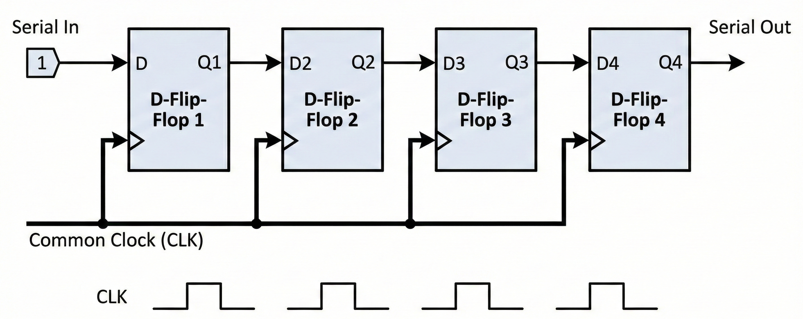
Tracing the Bit Movement
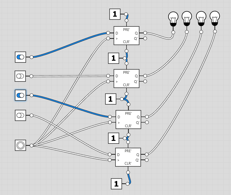
Let's see what happens if we input a single "1" and then keep the input at "0". This creates a "pulse" that travels through the register.
The Setup:
- Flip-Flops: 4 (Q1, Q2, Q3, Q4)
- Common Clock: All connected together.
- Input: Connected only to Q1.
State Table
Watch how the "1" moves one step to the right on every Rising Edge of the clock.
| Clock Pulse | Serial Input | Q1 | Q2 | Q3 | Q4 | Comment |
|---|---|---|---|---|---|---|
| Start | 1 | 0 | 0 | 0 | 0 | Input is ready, but door is locked. |
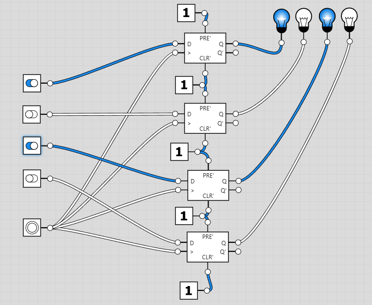
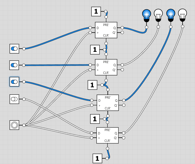
| Pulse 1 | 0 | 1 | 0 | 0 | 0 | Load: Q1 grabs the input. |
| Pulse 2 | 0 | 0 | 1 | 0 | 0 | Shift: Q2 grabs Q1's value. |
| Pulse 3 | 0 | 0 | 0 | 1 | 0 | Shift: Q3 grabs Q2's value. |
| Pulse 4 | 0 | 0 | 0 | 0 | 1 | Shift: Q4 grabs Q3's value. |
Visualizing the "Shift"
Here is a frame-by-frame view of the Flip-Flops. Notice how the Green Box (Logic 1) hops to the right.
Look at the "Serial Input" column. After Pulse 1, we changed the input to 0. So when Pulse 2 happened, Q1 grabbed that 0, while passing its old 1 to Q2.
Hardware Activity: Build a 4-Bit Shift Register
We will modify your previous circuit. We don't need 4 switches anymore—just one!
Components:
- 2x 7474 Dual D Flip-Flop ICs (Total 4 Flip-Flops)
- 1x Push Button (Data Input)
- 1x Push Button (Clock)
- 4x LEDs (Outputs)
Wiring Changes:
- Keep Power & Clock: Leave the power and the common clock line exactly as they were from the Parallel Register.
- Daisy Chain the Data:
- Input: Connect your Data Button to Chip 1, Pin 2 (D1).
- Link 1: Connect Chip 1, Pin 5 (Q1) to Chip 1, Pin 12 (D2).
- Link 2: Connect Chip 1, Pin 9 (Q2) to Chip 2, Pin 2 (D3).
- Link 3: Connect Chip 2, Pin 5 (Q3) to Chip 2, Pin 12 (D4).
- Outputs: Ensure LEDs are connected to all Q pins (Pins 5 and 9 on both chips).
Test It:
- Reset: Cycle the clock until all LEDs are OFF.
- Load: Hold the Data Button (Input=1). Press Clock ONCE. (LED 1 turns ON).
- Shift: Release the Data Button (Input=0). Press Clock again. (LED 1 OFF, LED 2 ON).
- Repeat: Keep pressing Clock and watch the bit travel to the end!
3) Part 3: Serial-to-Parallel Display
We have built two powerful circuits:
- Shift Register: Moves data down a single wire (Serial).
- Parallel Register: Grabs data all at once (Parallel).
Now, let's combine them to solve a real-world problem. Imagine you have a microcontroller (like an Arduino) that wants to control a display, but it only has 1 wire available. How do you send a 4-bit number (like "9" or 1001) over 1 wire?
The Strategy:
- Load: Send the bits one by one into a Shift Register (using 4 clock pulses).
- Latch: Once all 4 bits are in position, trigger a Parallel Register to "grab" them and show them on the display.
This is exactly how modern display drivers work!

Components You'll Need
- Shift Stage: 2x 7474 Dual D Flip-Flops (chained as Shift Register)
- Storage Stage: 2x 7474 Dual D Flip-Flops (wired as Parallel Register)
- Decoder: 1x 74LS48 BCD Decoder
- Display: 1x 7-Segment Display (Common Cathode)
- Inputs: * 1x Data Button (Serial Input)
- 1x Shift Clock Button
- 1x Latch Clock Button
Step-by-Step Assembly
Step 1: Build the Shift Register (The Bucket Brigade) (If you still have your circuit from Part 2, keep it!)
- Chain 4 flip-flops (Q -> D) as done in the previous section.
- Connect all their Clock pins to the Shift Clock Button.
- Connect the first D input to the Data Button.
Step 2: Build the Storage Register (The Camera)
- Place two new 7474 ICs (or reuse if you have a large breadboard).
- Connect the D Inputs of this new register to the Q Outputs of the Shift Register.
- Shift Q1 -> Storage D1
- Shift Q2 -> Storage D2
- ...and so on.
- Connect all Clock pins of the Storage Register to a separate button: the Latch Clock.
Step 3: Connect the Display
- Connect the Q Outputs of the Storage Register to the inputs (A, B, C, D) of the 74LS48 Decoder.
- Wire the 74LS48 to the 7-Segment Display as usual.
The Operation (How to use it)
Let's display the number 5 (0101).
- Clear: Ensure the display is showing something old (random).
- Serial Loading (The Secret Work):
- Bit 1 (1): Hold Data=1. Press Shift Clock. (Shift Reg has: 1000)
- Bit 2 (0): Release Data=0. Press Shift Clock. (Shift Reg has: 0100)
- Bit 3 (1): Hold Data=1. Press Shift Clock. (Shift Reg has: 1010)
- Bit 4 (0): Release Data=0. Press Shift Clock. (Shift Reg has: 0101)
- Notice: The display has NOT changed yet! The data is hidden inside the shift register.
- The Reveal:
- Press the Latch Clock button ONCE.
- Boom! The Storage Register grabs 0101, sends it to the decoder, and the number "5" appears instantly on the screen.
If we connected the display directly to the Shift Register, the user would see flickering garbage numbers (1, 2, 5...) while the data was moving. The Storage Register freezes the image so the display is stable during loading.
In the next section, we will do an exciting project on design of clocks using flip-flops.